Logic Gate Commutation PCB Part 1
Now its time to get started on the fun stuff. That is circuit design and layout. This will be just encompassing the gate logic commutation circuits, PWM circuit, MOSFETs, gate drivers, and power supplies. I will be dedicating a section in this post to each of these circuits. This is just a basic circuit meant to spin the motor both ways with logic gates. There will be no load so the design should be pretty simple. There will be cases were if it were going to do more than just spin I would add extra circuits or safety margin. That not being the case this board will be pretty simple.
Logic Gate Commutation
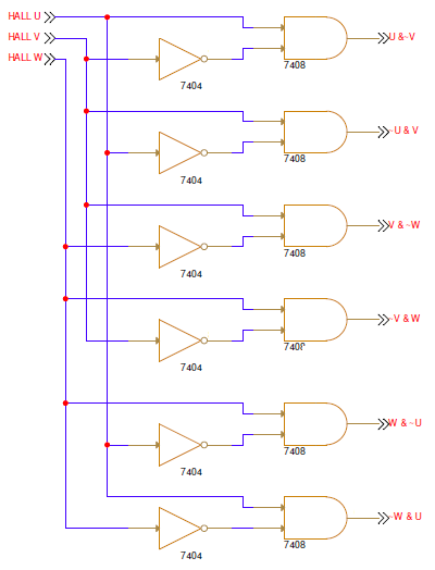
As shown in the previous post and table below only 6 signal combinations need to be created with the hall sensors. Clockwise and counter clockwise directions use similar ones. The only exception being the HIGH and LOW signales to the gates are switched.
| FET GATE | CW EQUATION | CWW EQUATION |
|---|---|---|
| HIGH U | HALL U & !HALL V | !HALL U & HALL V |
| LOW U | !HALL U & HALL V | HALL U & !HALL V |
| HIGH V | HALL V & !HALL W | !HALL V & HALL W |
| LOW V | !HALL V & HALL W | HALL V & !HALL W |
| HIGH W | HALL W & !HALL U | !HALL W & HALL U |
| LOW W | !HALL W & HALL U | HALL W & !HALL U |
Using this info we can just reuse the circuits from the previous posts. Since I am creating a PCB myself I want it to look sleeker. I have decided to use SMD parts were possible. All the logic 7400 components will be surface mount. Look at circuit below and previous posts for more detail.
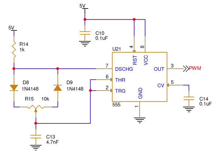
PWM Circuit
This is going to be a resuse of the circuit I used before there will not be any changes. With the exception that I am going to use surface mount parts and they will be on a PCB versus on a breadboard. Look up the datasheet on a 555 or other websites that have further explanations of the 555 timer. The circuit is below.
CW or CCW Circuit
As shown above the equations for the HIGH and LOW gates for each phase are just reveresed when going in the oposite direction. In the spirit of 7400 series I chose to use 74157 multiplexer. There will be a switch connected to the multiplexer that will select to either use the CW or CCW commutation equations. A switch will be connected to ground or 5V depending on the direction. This is a newer circuit look at the circuit below.
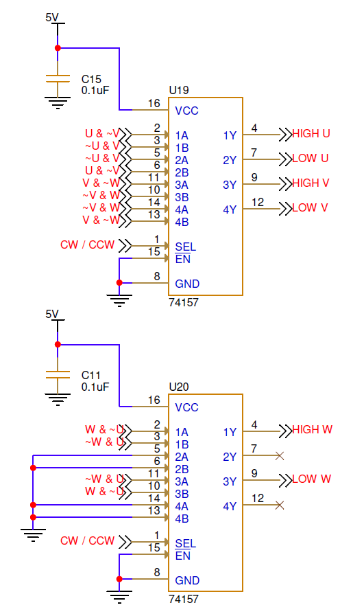
The operation of this circuit is given in the datasheet. As you can see depending on the select line it will either output A or B. Having all clockwise signals go to A and all counterclockwise signals to B inputs we can control for direction with one signal. This is what I got from the table.
| SELECT | INPUT A | INPUT B | OUTPUT Y |
|---|---|---|---|
| LOW | LOW | DOESN’T MATTER | LOW |
| LOW | HIGH | DOESN’T MATTER | HIGH |
| HIGH | DOESN’T MATTER | LOW | LOW |
| HIGH | DOESN’T MATTER | HIGH | HIGH |
Having the SELECT line connected to a switch with one pole to ground and the other to 5V, we can get change direction. That is all that is neded for changin directions.
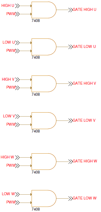
Combining PWM with Gate Signals
This is similar to the previous posts. Just using an AND gate for PWM output from the 555 timer (for duty cycle) and each gate signal. Same 7408 IC will be used as the Logic Gate Commutation schematic. Looking at the signals delay being in the 10s of nanoseconds should not effect the perfromance of the PWM or turn on. The minimum PWM cycle at 1% would be 20kHz * 1% = 500ns. The datasheets for the 7400 series has a delay of at most 30ns. This should be fine for this application. Our PWM will not even be this low because of the 555 timer. I can probably optamize it for that kind of tolerance, but no need for it.
MOSFETs
Picking a MOSFET for a motor driver requires info on the motor. The motor I am going to use is Linix 45ZWN24. According to the datasheet its rated voltage is 24V and curre t is 2.4A. I like going on Digikey or Mouser and start putting in parameters that I know. First will start with the simple parameter voltage. VDSS is the breakdown of the FET from drain to source. A good rule of thumb is to pick a FET with 2x the voltage you will be applying to the motor. You don’t want to pick the highest VDSS, because the higher the VDSS the higher RDSON and GC will be. These will impact other performance issues. With the motor being rated for 24V I will be looking for a 2 x 24V = 48V rated part. Looking for VDSS common values it shows that 55V or 60V are common VDSS values. That is what I entered to look for. Next parameter I need to look for is current. I doubled up the current for continuous. That is 2.4A x 2 = 4.8A. Looking through datasheets making sure the part can handle 4.8A conitinuous and 9.6A peak. This should be more than enough. I would be more exact if I had more motor parameters, but the datasheet is limited in info. Next important parameters for me were pricing and SMD footprints. I do not want a part I can’t solder. I picked out some parts and started looking at RDSON, power dissipation, and gate capacitance. Toshiba TPH9R506PL seemed to be a part I liked the most. So lets take a look at its RDSON.
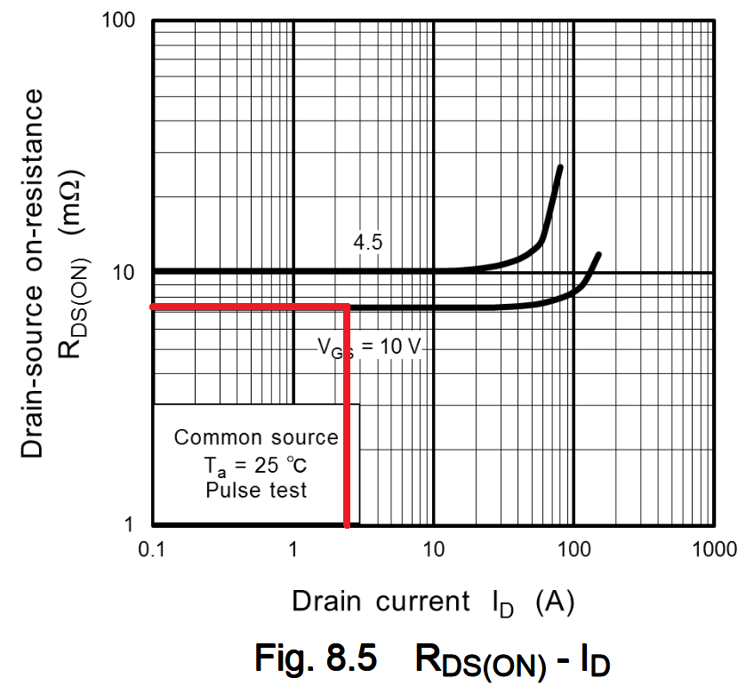
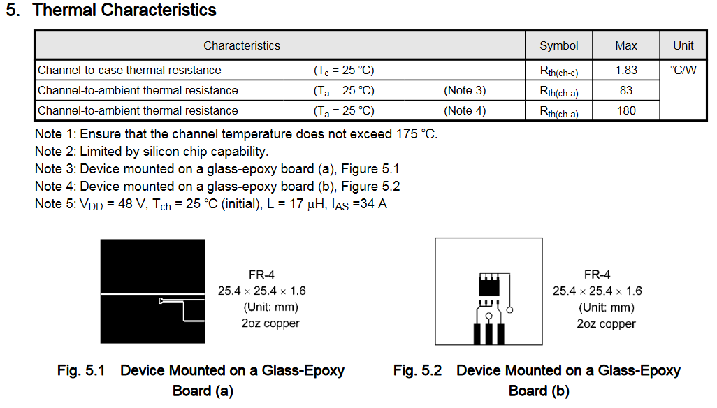
From the graph we can see that at 2.4A the RDSON will be 7.3mOhms. With this we can take a look at how much power dissipation will be effected. Formula for power dissipation is I2R = 2.4 * 2.4 * 0.0073 = 0.042W. Now we got to look at what the part can safely dissipate. Looking a the parameters given in the datasheet I think we should be safe. The one with barely any copper can dissipate 0.83W. Yes, its 2 oz copper where I will be using 1 oz, but I will have bigger copper planes than that.
Every application is different and requires different parameters. You have to narrow down what is the most important for your project. These FETs will be more than adequate for this board.
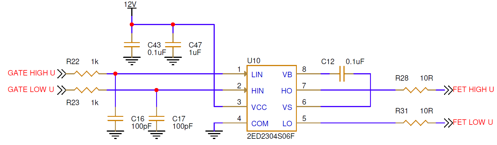
Gate Drivers
Now we have to take a look at properly turning on FETs. FETs might list a low turn on voltage (4.5V in this case), but for most applications you want to go way above that. That guarantees a turn on and has better values for RDSON. We know we need a high and low side driver, takes 5V logic, 12V for power, and be ok for 24V on the FET side (they will produce 36V for the gates of the high MOSFETs). The other important aspect of this is the current driving capabilities. There is more than one way to do this. I am going to use the simpler method. All we need is the FETs total gate charge and rise/fall times. Gate charge is given as 21nC at 10V. Rise/fall time is a parameter we need for this design. As said before in the 555 timer section, the switching frequency is 20kHz. With 1% being 500ns. Lets say we probably want to be 1/5th of the time in rising edge. This would be 100ns. I will take this as the minimum rise / fall time.
Igate = Qtotal / Trise 21nC / 100nS = 0.21A
With this and the current IC market being tight I choose the Infineon 2ED2304S06F. Next the bootstrap capacitor has to be choosen. Some datasheets provide the info to choose one. This one does not. Bootstrap capacitor should be about 50 times the required gate charge at your operating voltage. 12V in our case.
Cbootstrap = Qgate / Vbootstrap * 50 21nC / 12V * 50 = 87.5 nF
If this will be deemed to small I can always increase it. A 0.1uF will be used since it is a pretty common value. The other capacitor that needs to be caluclated is the bulk capacitor for the driver. A good rule of thumb I have noticed is 10x the bootstrap capaciotr. In this case it will be 1uF. If there will be issues we can measure and change it.
For the gate series resistor a good starting point is taking current required for rise/fall time. Next taking the voltage that will be present on the gate. Taking this info a rough starting point can be figured out.
Rgate = Vgate / Igate 12V / 0.21A = 57Ohms
Closest common value is 56Ohms. That is what will be chosen for this design. Another good practice is to add a diode and resistor in parrallel to this gate series resistor. The 56Ohms resistor will be used for charging and the diode with resistor will be used for discharging. Usually you want the FETs to turn off faster than to turn on. Trying to keep this board simple, I will not be adding the diode and resistor in parallel.
Inverter
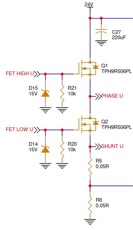
Having the calculated driver components I put them togather in the circuit below. I also included a little filter on the inputs to the gate driver. Also added a 15V zener and pull down resistor just in case.
Power Supplies
I used some parts I already have in my parts library. I am using a 5V LDO with 150mA output which will be enough for the logic circuits. For the 12V power supply I am using also and LDO with 500mA of output. This should be adeqaute since only two FETs will be on and the output currents are not continuous. I also have spares of these parts.
Next Time
Thats it for this post. Next post I will be going over my layout and hopefully ordering boards. After these boards will be built and tested I will move on to laying out a board with a micro. That way more fun can be had with it. If there is something I did wrong let me know so I can fix it.